
淺談 Digital IC Back-end Process
05/28/2022 Tags: EDA Miscellaneous“Platform-based systems typically consist of a basic RISC processor, which can be extended with multipliers, floating point units, or specialized DSP units. RISC processor core can have an HDL model that describes the behavior of the processor; a gate netlist that describes the type and interconnection of gates required to produce the processor; and a placement and routing description that describes how to physically build the processor in a given process.”
“Modern versions of the venerable “silicon compiler” can be built in a structured hierarchical manner to generate memories, register files, and other special-purpose structures that can benefit from a customized layout. One of the most straightforward approaches is to write custom placement routines that in essence “hand place” certain standard cells within the row structure of a standard cell design.”
簡介
Digital IC Back-end Process 屬於VLSI設計的其中一個環節,這篇文章的內容來源主要是參考原文書,將部分內容整理在這邊,以便於閱讀以及回顧。
Automated Layout Generation
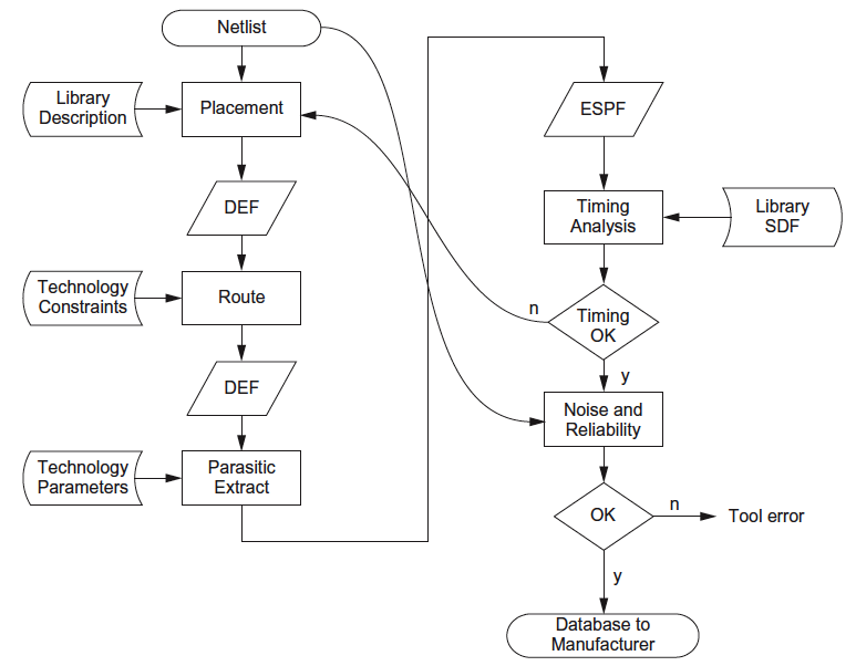
Placement and Routing
- “Layout generation is the last step in the process of turning a design into a manufacturable database. It transforms a design from the structural to the physical domain.”
- “The netlist might be provided in the Design Exchange Format (DEF) as a Verilog netlist.”
- “The placement tool takes a standard cell library definition describing cell dimensions and port locations, typically in the Library Exchange Format (LEF).”
- “The objective of a simple placement algorithm is to minimize the length of wires.”
- “At the end of the placement phase, the cells have been fixed in position in the overall array.”
- “The placed design is saved in a standard format (e.g., DEF) for routing. After placement of cells, the signal nets in the circuit need to be routed.”
- “Routing is normally divided into two steps: global routing and detailed routing.”
- “The placed and routed design is then passed to the circuit parasitic extractor.”
- “The placed and routed design is provided to the extractor in DEF format and the output is an Extended Standard Parasitic Format (ESPF), Reduced Standard Parasitic Format (RSPF), or Standard Parasitic Exchange Format (SPEF) that describes the R’s and C’s associated with all nets in the layout”
Timing Analysis
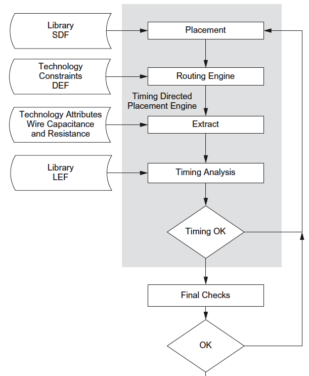
- Multiple iterations of synthesis and placement & routing are usually necessary to converge on timing requirements.
- The trouble with a place-then-route strategy is that after the layout is completed, the parasitic routing capacitance is extracted and the timing analysis is done to estimate timing.
- The solution is to use a technique called timing-driven placement, which takes into account the timing (speed) of the circuit as cells are placed.
<Note> The support costs amortized over the life of the equipment and the length of the design that might break down as project include:
- Computer costs: $10K
- CAD Tools (digital front end): $10K
- CAD Tools (analog): $100K
- CAD Tools (digital back end): $1M
- Education or re-education costs: $10–$30K
Example:
You are starting a company to commercialize your brilliant research idea. Estimate the cost to prototype a mixed-signal chip in a 45 nm process. Assume you have seven digital designers, three analog designers, and five support personnel and that the prototype takes two fabrication runs and two years.
Assume that seven digital designers will cost 7 X ($70K + $30K + $10K + $10K) = $840. The three analog designers will cost 3 X ($100K + $30K + $10K + $100K) = $720K. The five support personnel cost 5 X ($40K + $20K + $10K) = $350K. One fabrication run with the back-end tools will cost $6M. Thus, the cost is $7.91M per year.
=========== To be continued…. ==========
Reference
- CMOS VLSI Design A Circuits and Systems Perspective
Thanks for reading! Feel free to leave the comments below or email to me. Any pieces of advice or discussions are always welcome. :)